
The ATmega328p has two 8 bit timers and one 16 bit timer. Each timer has multiple modes of working. We will be covering all the timers together in the tutorial, one mode at a time.
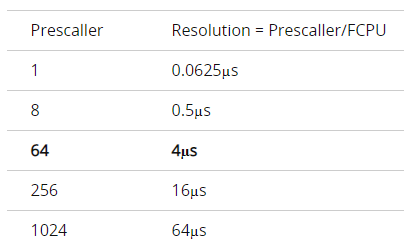
Timers & Prescalers
A timer is a specialized type of clock used to measure time intervals. It maintains the timing of an operation in sync with a system clock or an external clock. The purpose of the Prescaler is to allow the timer to be clocked at the rate a user desires.
Normal Mode – Timer 0/2
The simplest mode to mess around with, the timer starts from BOTTOM (0x00) and goes all the way to the MAX/TOP (0xFF) and overflows back to the BOTTOM (0x00). When the timer overflows it maybe programmed to generate an Timer Overflow Interrupt.
In normal operation the Timer/Counter Overflow Flag (TOV0) will be set in the same timer clock cycle as the TCNT0 becomes zero. The TOV0 Flag in this case behaves like a ninth bit, except that it is only set, not cleared. However, combined with the timer overflow interrupt that automatically clears the TOV0 Flag, the timer resolution can be increased by software. There are no special cases to consider in the Normal mode, a new counter value can be written anytime.
The normal mode can be used to do tasks at regular intervals of time, logging data from sensors, monitoring the status of battery and many such activities . The time period between two interrupts in the normal mode can be set using the appropriate prescaler and load value. For the sake of this example, let us consider a situation where we are supposed to toggle D13 every one second. Assuming FCPU = 16 MHz, the resolution can be calculated using:
Resolution = Prescaler/FCPU
Using an initial load value of 6, will give us 250 counts before an overflow occurs. Therefore with a prescaler of 64 it takes 1000us for each overflow to occur. Using a software counter to keep track of overflows, we can see that 1000 overflows would take 1 second. The below example shows how to do the same through programming.
1
2
3
4
5
6
7
8
9
10
11
12
13
14
15
16
17
18
19
20
21
22
23
24
25
26
volatile long count = 0;

ISR(TIMER2_OVF_vect) {
  TCNT2 = 6;
  if (count >= 1000){ // 1 second
    PORTB ^= (1 << 5); //toggle D13
    count = 0;
  }
  else {
    count++;
  }
}

void setup(){
  pinMode(13, OUTPUT);
  cli(); //Disable Global Interrupts
  TCCR2A = 0; //Normal Mode
  TCCR2B = 0;
  TIMSK2 |= (1 << TOIE2); //Enable overflow interrupt
  sei(); //Enable Global Interrupts
  TCNT2 = 6; //Load value
  TCCR2B |= (1 << CS22); // Prescaler set to 64
}

void loop(){
}
Normal Mode – Timer 1
The normal mode for timer 1 is very similar to normal mode of timer 2/0, the only difference being the step count which arises due to the 8 and 16 bit values of the timers.
The counter simply overruns when it passes its maximum 16-bit value (MAX = 0xFFFF) and then restarts from the BOTTOM (0x0000). In normal operation the Timer/Counter Overflow Flag (TOV1) will be set in the same timer clock cycle as the TCNT1 becomes zero. The TOV1 Flag in this case behaves like a 17th bit, except that it is only set, not cleared. However, combined with the timer overflow interrupt that automatically clears the TOV1 Flag, the timer resolution can be increased by software. There are no special cases to consider in the Normal mode, a new counter value can be written anytime.
CTC Mode – Timer 0/2
In the normal mode we had to reset the timer after each overflow to a load value, this is a very inefficient way of generating a waveform as writing into TCNTn is an software level change which uses the CPU resources and also its a lot slower than a hardware level change.
Enter CTC mode, where the timer starts from the BOTTOM (0x00) and counts till it reaches the TOP which is equal to OCRnA and NOT MAX(0xFF). The OCRnA defines the top value for the counter, hence also its resolution. This mode allows greater control of the compare match output frequency. It also simplifies the operation of counting external events. An interrupt can be generated each time the counter value reaches the TOP value by using the OCF2A Flag. If the interrupt is enabled, the interrupt handler routine can be used for updating the TOP value.
For generating a waveform output in CTC mode, the OCnA output can be set to toggle its logical level on each compare match by setting the COMnA bits. The OCnA value will not be visible on the port pin unless the data direction for the pin is set to output. As for the Normal mode of operation, the TOVn Flag is set in the same timer clock cycle that the counter counts from MAX to BOTTOM(0x00).
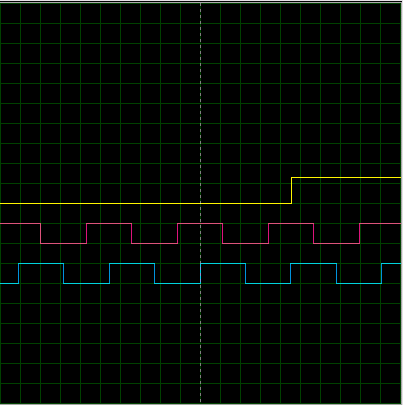
Lets take up the example from normal mode, and add a few more features to it. Lets generate three different waveforms, a 500 Hz wave by toggling the OCnA pin, another 500 Hz wave using the TIMERn_COMPA_vect and finally a 0.5 Hz wave using a software prescaler present insider the Interrupt handle like we did in the normal mode.
1
2
3
4
5
6
7
8
9
10
11
12
13
14
15
16
17
18
19
20
21
22
23
24
25
26
27
28
29
30
31
32
volatile long count = 0;

ISR(TIMER2_COMPA_vect) {
  PORTB ^= (1);
  if (count >= 1000) {
    count = 0;
    PORTB ^= (1 << 5);
  }
  else {
    count++;
  }
}

void setup() {
  pinMode(13, OUTPUT);
  pinMode(11, OUTPUT);
  pinMode(8, OUTPUT);
  cli();
  TCCR2A = 0;
  TCCR2A |= (1 << COM2A0) | (1 << WGM21); //toggle OCR2A & CTC Mode
  TCCR2B = 0;
  TCNT2 = 0;
  OCR2A = 249; // Clear Compare value
  TIMSK2 |= (1 << OCIE2A); //enable Output Compare Interrupt
  sei();
  TCCR2B |= (1 << CS22); //Prescaler set to 64
}

void loop() {
  // put your main code here, to run repeatedly:

}
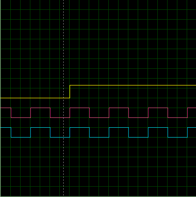 Yellow – D13, Pink – D8, Blue – D11
Although this program does get the job done, it’s not the most efficient way to get the task done. The 500 Hz wave generated by TIMER2_COMPA_vect is a software triggered wave, meaning the CPU is involved in the process which can be a problem in CPU intensive sketches.
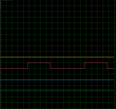
We will be writing a better version of the same code using both the output compare units instead of just OCRnA, here the OCnB pin is toggled directly through hardware which frees up the CPU.
Let’s generate three different waveforms, a 500 Hz wave by toggling the OCnA pin, another 500 Hz wave using the OCnB pin and finally a 0.5 Hz wave using a software prescaler present insider the Interrupt handle like we did in the normal mode. Another added feature would be the fact that OCRnB can be used to create a phase shift between the two 500 Hz waves.
1
2
3
4
5
6
7
8
9
10
11
12
13
14
15
16
17
18
19
20
21
22
23
24
25
26
27
28
29
30
31
32
volatile long count = 0;

ISR(TIMER2_COMPA_vect) {
  if (count >= 1000) {
    count = 0;
    PORTB ^= (1 << 5);
  }
  else {
    count++;
  }
}

void setup() {
  pinMode(13, OUTPUT);
  pinMode(11, OUTPUT);
  pinMode(3, OUTPUT);
  cli();
  TCCR2A = 0;
  TCCR2A |= (1 << COM2A0) | (1 << COM2B0) | (1 << WGM21); //toggle OCR2A,OCR2B & CTC Mode
  TCCR2B = 0;
  TCNT2 = 0;
  OCR2A = 249; // Compare value
  OCR2B = 100; // Compare value
  TIMSK2 |= (1 << OCIE2A); //enable Output Compare Interrupt
  sei();
  TCCR2B |= (1 << CS22); //Prescaler set to 64
}

void loop() {
  // put your main code here, to run repeatedly:

}
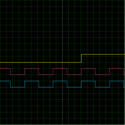
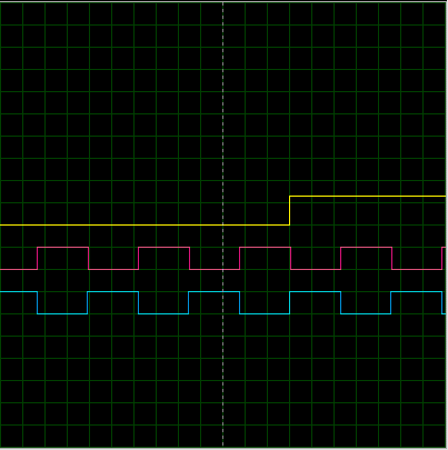
The phase shift between OCnA and OCnB can be seen in the above pictures.
Notice that all the examples we have discussed till now in CTC mode are for 50% duty cycle.
Finally before we switch to the next mode let us see how we can generate a 50 Hz PWM signal having 40% duty cycle using CTC mode.
1
2
3
4
5
6
7
8
9
10
11
12
13
14
15
16
17
18
19
20
21
22
23
volatile long count = 0;

ISR(TIMER2_COMPA_vect) {
  count++;
  OCR2A = count % 2 == 0 ? 2 : 1;
}

void setup() {
  pinMode(11, OUTPUT);
  cli();
  TCCR2A = 0;
  TCCR2A |= (1 << COM2A0) | (1 << WGM21);
  TCCR2B = 0;
  TCNT2 = 0;
  OCR2A = 1;
  TIMSK2 |= (1 << OCIE2A);
  sei();
  TCCR2B |= (1 << CS22); //pre
  // put your setup code here, to run once:
}

void loop() {
  // put your main code here
 D11 – Pink
Force Output Compare
In non-PWM Waveform Generation modes, the match output of the comparator can be forced by writing a one to the Force Output Compare (FOCnx) bit. Forcing compare match will not set the OCFnx Flag or reload/clear the timer, but the OCnx pin will be updated as if a real compare match had occurred (the COM11:0 bits settings define whether the OCnx pin is set, cleared or toggled).
Input Capture Unit
The Timer/Counter incorporates an Input Capture unit that can capture external events and give them a timestamp indicating time of occurrence. The external signal indicating an event, or multiple events, can be applied via the ICP1 pin or alternatively, via the analog-comparator unit. The time-stamps can then be used to calculate frequency, duty-cycle, and other features of the signal applied. Alternatively the time-stamps can be used for creating a log of the events.
When a change of the logic level (an event) occurs on the Input Capture pin (ICP1), alternatively on the Analog Comparator output (ACO), and this change confirms to the setting of the edge detector, a capture will be triggered. When a capture is triggered, the 16-bit value of the counter (TCNT1) is written to the Input Capture Register (ICR1). The Input Capture Flag (ICF1) is set at the same system clock as the TCNT1 value is copied into ICR1 Register. If enabled (ICIE1 = 1), the Input Capture Flag generates an Input Capture interrupt. The ICF1 Flag is automatically cleared when the interrupt is executed. Alternatively the ICF1 Flag can be cleared by software by writing a logical one to its I/O bit location.
The ICR1 Register can only be written when using a Waveform Generation mode that utilizes the ICR1 Register for defining the counter’s TOP value. In these cases the Waveform Generation mode (WGM13:0) bits must be set before the TOP value can be written to the ICR1 Register. When writing the ICR1 Register the high byte must be written to the ICR1H I/O location before the low byte is written to ICR1L.
CTC Mode – Timer 1
The CTC Mode for timer 1 is similar to the CTC mode available in timer 0/2, only difference being the option to use ICR1 as the top value other than the usual option to use OCR1A.
1
2
3
4
5
6
7
8
9
10
11
12
13
14
15
16
17
18
19
20
21
22
23
24
25
ISR(TIMER1_CAPT_vect) {
  TCCR1C |= (1 << FOC1A) | (1 << FOC1B);
}

void setup() {
  Serial.begin(9600);
  pinMode(9, OUTPUT); //OC1A
  pinMode(10, OUTPUT); //OC1B
  TCCR1A = 0;
  cli();
  TCCR1A |= (1 << COM1A0) | (1 << COM1B0); //toggle
  TCCR1B = 0;
  TCCR1B |= (1 << WGM12) | (1 << WGM13); // CTC+ICR
  TIMSK1 |= (1 << ICIE1); // Enable ICR interrupt
  TCNT1 = 0;
  ICR1 = 2039;
  OCR1A = 1223; //40% duty cycle
  OCR1B = 815; //60% duty cycle 815
  sei();// Enable Global Interrupts
  TCCR1B |= (1 << CS11); //8 prescaler
}

void loop() {
  // put your main code here, to run repeatedly:
}
Fast PWM
In the simplest PWM mode, The fast Pulse Width Modulation or fast PWM mode (WGM02:0 = 3 or 7) provides a high frequency PWM waveform generation option. The fast PWM differs from the other PWM option by its single-slope operation. The counter counts from BOTTOM to TOP then restarts from BOTTOM. TOP is defined as 0xFF when WGM2:0 = 3, and OCR0A when WGM2:0 = 7. In non-inverting Compare Output mode, the Output Compare (OC0x) is cleared on the compare match between TCNT0 and OCR0x, and set at BOTTOM. In inverting Compare Output mode, the output is set on compare match and cleared at BOTTOM.
The Timer/Counter Overflow Flag (TOV0) is set each time the counter reaches TOP. If the interrupt is enabled, the interrupt handler routine can be used for updating the compare value.
In fast PWM mode, the compare unit allows generation of PWM waveforms on the OC0x pins. Setting the COM0A1:0 bits to one allows the OC0A pin to toggle on Compare Matches if the WGM02 bit is set. This option is not available for the OC0B pin. The actual OC0x value will only be visible on the port pin if the data direction for the port pin is set as output. The PWM waveform is generated by setting (or clearing) the OC0x Register at the compare match between OCR0x and TCNT0, and clearing (or setting) the OC0x Register at the timer clock cycle the counter is cleared (changes from TOP to BOTTOM).
The PWM frequency for the output can be calculated by the following equation:
Frequency = fclock/(N*(TOP+1)) WHERE N IS THE PRESCALER.
Using OCRnA as the top value will give us more freedom in controlling the frequency of the output waveform, but OCRnA cannot be used both as the top value and the PWM compare value. Only OCRnB can be used to generate waveforms. However, there is a special-case mode “Toggle OCnA on Compare Match” that will toggle output A at the end of each cycle, generating a fixed 50% duty cycle and half frequency in this case.
1
2
3
4
5
6
7
8
9
10
11
12
13
14
15
16
17
18
19
void setup() {
  cli();
  TCCR2A = 0; //clear the values
  TCCR2A |= ((1<<COM2A1)|(1<<COM2B1)|(1<<WGM20)|(1<<WGM21)); // set to fast PWM with std TOP and use non-inverting mode for OCnA and OCnB
  TCCR2B = 0;
  pinMode(11,OUTPUT);
  pinMode(3,OUTPUT);
  OCR2A = 204; // 30% duty cycle
  OCR2B = 76; // 80% duty cycle
  TCCR2B |= (1<<CS22); //prescaler set to 64
  sei();
  // put your setup code here, to run once:

}

void loop() {
  // put your main code here, to run repeatedly:

}
Coming Up
- Phase Correct PWM
- Phase and Frequency Correct PWM